High-Sensitivity Detection with Graphene-Based Nanosensors

Introduction

The demand for advanced sensor technologies that offer ultra-sensitive and rapid detection of target analytes is growing across industries. From healthcare diagnostics to environmental monitoring, the ability to identify specific compounds or biomarkers with precision can dramatically improve outcomes and drive innovation. Our patented graphene-based nanosensor presents a cutting-edge solution, offering high sensitivity and specificity for detecting a wide range of target analytes in real-time. This technology is set to transform how industries approach monitoring and diagnostics by providing faster, more accurate detection with minimal sample sizes.

Limitations in Conventional Sensor Technologies

Traditional sensor technologies often struggle with sensitivity, particularly when dealing with extremely low concentrations of target analytes. This poses significant challenges in critical applications like early disease detection, environmental contaminant monitoring, and pharmaceutical development, where even minute amounts of a compound can be crucial. Many conventional sensors also lack the speed or adaptability needed to keep up with real-time monitoring, leading to delays in diagnosis or decision-making.

These limitations highlight the need for more advanced sensor systems that can operate efficiently at the nanoscale, providing highly accurate detection with faster turnaround times. In industries like healthcare, where early detection of diseases can be life-saving, more sensitive and specific sensors are essential.

Graphene: The Key to Enhanced Sensitivity

Our patented graphene-based nanosensor takes full advantage of graphene’s unique properties—its extreme thinness, conductivity, and high surface area—to detect target analytes with unparalleled sensitivity. The nanosensor is designed to interact with specific analytes, such as biomarkers for diseases, pollutants, or chemical compounds, allowing it to provide a rapid and precise signal when the target is present.

The versatility of graphene allows this nanosensor to be adapted for a wide variety of applications, from medical diagnostics to environmental testing. In the healthcare field, for example, the nanosensor can be used to detect biomarkers of diseases like cancer at very early stages, enabling timely interventions. Similarly, in environmental monitoring, the sensor can detect pollutants or hazardous materials at ultra-low concentrations, providing a powerful tool for protecting ecosystems and public health.

Why This Technology Stands Out

  • Unmatched Sensitivity: Graphene’s unique properties enable the sensor to detect even trace amounts of target analytes, ensuring high accuracy in critical applications.
  • Fast, Real-Time Detection: The nanosensor provides rapid results, making it ideal for applications where time is of the essence, such as medical diagnostics or environmental monitoring.
  • Wide Range of Applications: From healthcare to environmental science and consumer electronics, this technology can be adapted for numerous industries.
  • Scalable and Cost-Effective: The nanosensor’s design allows for scalability in production, making it feasible for widespread commercial use.

Setting a New Standard for Nanosensor Technology

Licensing this graphene-based nanosensor technology offers a unique opportunity to develop highly sensitive, rapid, and adaptable detection systems across multiple industries. As the demand for real-time, high-precision monitoring continues to rise, this technology presents a transformative solution for businesses seeking to lead in biosensing, diagnostics, and environmental protection.
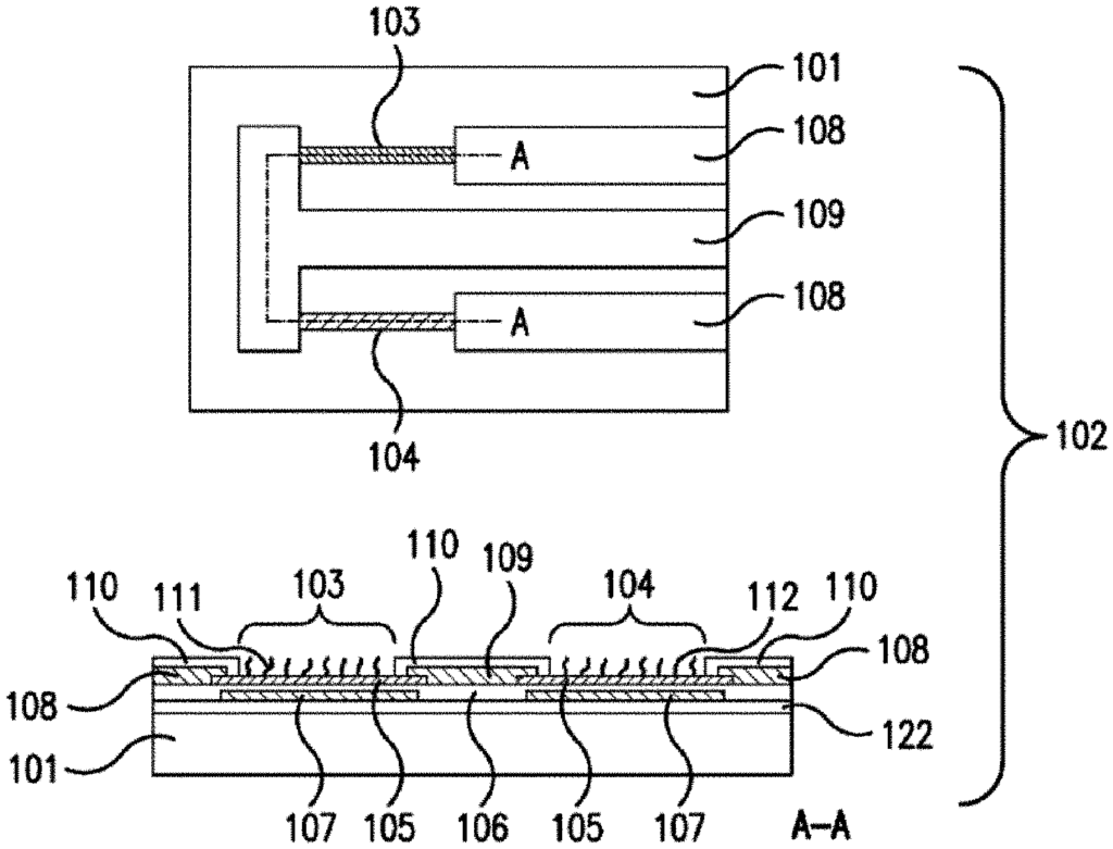
A microdevice for monitoring a target analyte is provided. The microdevice can include a field effect transistor comprising a substrate, a gate electrode, and a microfluidic channel including graphene. The microfluidic channel can be formed between drain electrodes and source electrodes on the substrate. The microdevice can also include at least one aptamer functionalized on a surface of the graphene. The at least one aptamer can be adapted for binding to the target analyte. Binding of the target analyte to the at least one aptamer can alter the conductance of the graphene.

1. A microdevice for monitoring a target analyte, the microdevice comprising:

a field effect transistor comprising:

a substrate;
a gate electrode; and
a microfluidic channel or a micro transducer including graphene formed between drain electrodes and source electrodes on the substrate; and
at least one aptamer functionalized on a surface of the graphene, wherein the at least one aptamer is adapted for binding to the target analyte, and wherein binding of the target analyte to the at least one aptamer can alter the conductance of the graphene,
wherein binding of the target analyte to the at least one aptamer causes a conformational change of the at least one aptamer, causing the target analyte to be brought into a proximity to the surface of the graphene.
2. The microdevice of claim 1, wherein the microfluidic channel or the micro transducer is bound to the substrate for analyte and buffer introduction to initiate association and dissociation of the target analyte to the at least one aptamer.
3. The microdevice of claim 1, wherein the field effect transistor further comprises a gate capacitor comprising of an electrical double layer formed at the interface of the graphene and the solution.
4. The microdevice of claim 1, wherein the target analyte being brought into proximity to the surface of the graphene causes electrical properties of graphene to change by at least one of charge transfer and electrostatic interaction.
5. The microdevice of claim 1, further comprising at least one of an on-chip temperature sensor and a Peltier module to perform closed-looped temperature control of the microdevice.
6. The microdevice of claim 1, wherein the microdevice is configured to provide a label-free direct characterization of biomolecular binding properties with one-step electrical readout.
7. The microdevice of claim 1, wherein binding of the target analyte to the aptamer causes a carrier concentration in the graphene to be altered, resulting in a detectable signal.
8. The microdevice of claim 1, wherein the at least one aptamer is functionalized on the surface of the graphene using a linker, wherein the linker is configured to be irreversibly attached to the graphene without altering electronic properties of the graphene.
9. The microdevice of claim 8, wherein the at least one aptamer is directly attached to the linker by forming an amide bond.
10. The microdevice of claim 8, wherein the linker can be coupled to the graphene via stacking, and wherein the at least one aptamer can be attached to the free end of linker by forming an amide bond.
11. The microdevice of claim 8, wherein the linker comprises 1-pyrenebutanoic acid succinimidyl ester (PASE).
12. The microdevice of claim 1, wherein the field effect transistor further comprises a source electrode and a drain electrode, and wherein the graphene makes contact with both the source electrode and the drain electrode.
13. The microdevice of claim 1, wherein the graphene comprises a single layer sheet.
14. The microdevice of claim 1, wherein the target analyte is disassociated from the at least one aptamer by introducing a buffer to the at least one aptamer.

15. A method for monitoring a target analyte using an aptamer capable of binding to a target analyte, comprising:

placing a nanosensor in contact with target analytes, wherein the nanosensor comprises a first conductance element functionalized with an aptamer configured to detect the target analyte and a second conductance element that is insensitive to the target analyte;
detecting a difference, if any, in the conductance of the first and second conductance elements; and
based on the detected difference, determining a presence of the target analyte.
16. The method of claim 15, wherein the binding of the aptamer with the target analyte causes a change in the charge density on the first conductive element surface.
17. The method of claim 15, wherein a differential measurement of the conductance of the first conductance element and the second conductive element provides for determination of the presence of the target analyte and reduces an environmental factor.
18. The method of claim 15, wherein a surface of the first conductance element is adapted for a change in charge density thereon upon the binding of the aptamer with the target analyte.
19. The method of claim 15, wherein the nanosensor is adapted for real-time detection of a target analyte concentration.
20. The method of claim 15, wherein the real-time detection is continuous over time.
21. The method of claim 19, wherein the target analyte concentration is a physiologically relevant concentration.
22. The method of claim 15, further modifying the aptamer to adjust a specificity of the nanosensor to the target analyte.
23. The method of claim 22, wherein the target analyte includes an insulin.
24. The microdevice of claim 1, wherein a specificity of the microdevice to the target analyte is adjusted by modifying the aptamer.
25. The microdevice of claim 1, wherein the conformational change of the at least one aptamer includes parallel G-quadruplex conformation and antiparallel G-quadruplex conformation.
26. The microdevice of claim 1, wherein the at least one aptamer comprises a guanine-rich IGA3 aptamer or a synthetic single-stranded DNA VR11 aptameter.
27. The microdevice of claim 11, wherein the aptamer is coupled to the PASE through a reaction of an amino group of the aptamer with N-hydroxysuccinimide ester of PASE.
28. The microdevice of claim 1, wherein the microdevice is adapted for real-time detection of changes in the target concentration.
29. The microdevice of claim 28, wherein the real-time detection is continuous over time.
30. The microdevice of claim 1, wherein the substrate of the field effect transistor comprises Silicon (Si) and/or Silicon Dioxide (SiO2).
31. The microdevice of claim 1, wherein the substrate of the field effect transistor comprises flexible materials, wherein the flexible materials comprise Polyethylene Terephthalate (PET) or Biaxially-Oriented Polyethylene Terephthalate (Mylar).
32. The microdevice of claim 31, wherein the microdevice maintains consistent mechanical properties through cyclic rolling, twisting, and/or stretching deformations, wherein the mechanical properties include flexibility, durability, or elasticity.
33. The microdevice of claim 31, wherein the microdevice maintains consistent electrical properties through cyclic rolling, twisting, and/or stretching deformations, wherein the electrical properties include transconductance, carrier mobility, or on/off ratio.

Share

Title

Graphene-based nanosensor for identifying target analytes

Inventor(s)

Qiao Lin, Yibo Zhu, Junyi Shang, Zhixing Zhang, Xuejun Wang, Jaeyoung YANG, Cheng Wang, Pavana G. Rotti, John F. Engelhardt, Zhuang Hao

Assignee(s)

Department Of Anatomy And Cell Biology University Of Iowa, Columbia University in the City of New York

Patent #

20200196925

Patent Date

June 25, 2020

Inquire about this intellectual property

Learn more about "High-Sensitivity Detection with Graphene-Based Nanosensors"