Precision Nanoparticle Handling with Electrostatic Trapping Technology

Introduction

Nanoparticles are critical to the future of science and technology, with applications spanning medicine, electronics, and environmental science. However, their minuscule size presents unique challenges in terms of handling, manipulation, and isolation. Traditional methods of capturing and studying nanoparticles often lack the precision required for high-stakes applications like drug delivery, semiconductor manufacturing, or environmental monitoring. Our patented nanoparticle electrostatic trap offers a solution to these challenges by enabling precise, non-invasive capture and manipulation of nanoparticles with unprecedented accuracy.

Limitations in Current Nanoparticle Handling Methods

Nanoparticles are central to many technological advances, but their small size and unique properties make them difficult to isolate and manipulate using conventional methods. Techniques such as centrifugation or filtration can cause contamination, damage, or even loss of the particles during handling. For industries relying on the purity and precise positioning of nanoparticles, such as semiconductor manufacturing or targeted drug delivery, these inefficiencies present major obstacles.

The need for a more accurate and controlled approach to isolating nanoparticles is critical across several fields. Whether it’s collecting nanoparticles from the environment for pollution analysis or precisely positioning them in electronic components, industries need tools that can offer better control over these tiny materials.

Electrostatic Trapping: A Game-Changer for Nanoparticle Control

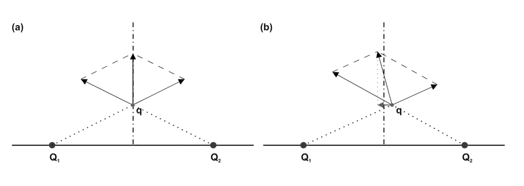
Our patented nanoparticle electrostatic trap provides a solution to the problem of handling and manipulating nanoparticles. This technology utilizes an electrostatic field to trap and hold nanoparticles without the need for physical contact. This non-invasive method ensures that nanoparticles remain pure and undamaged, making it ideal for applications requiring high precision.

The versatility of the electrostatic trap means that it can be used across a range of industries. In semiconductor manufacturing, it can improve the precision with which nanomaterials are placed onto substrates, leading to better-performing electronic devices. In biotechnology, it allows for the isolation of biological nanoparticles like proteins, viruses, or DNA fragments, supporting advanced research and development of therapies. Environmental scientists can use it to capture nanoparticles from the air or water, enabling more accurate monitoring of pollution levels and sources.

Key Advantages of the Technology

  • Non-Contact Handling: Electrostatic trapping allows for precise control over nanoparticles without physical interference, preventing damage or contamination.
  • Versatile Applications: From biotechnology to semiconductor manufacturing, this technology can be used in a wide variety of fields where nanoparticle manipulation is critical.
  • Improved Precision: The system allows for highly accurate isolation and positioning of nanoparticles, enhancing performance in applications where precision is paramount.
  • Scalability: The electrostatic trapping method can be adapted for both small-scale research and large-scale industrial applications.

Unlocking New Potential in Nanotechnology

Licensing this nanoparticle electrostatic trap technology offers businesses a powerful tool to lead in fields where nanoparticle manipulation is essential. By providing non-invasive, highly precise control over nanoparticles, this technology has the potential to improve processes in biotechnology, environmental monitoring, and semiconductor manufacturing, delivering both immediate benefits and long-term innovation.

A method of trapping a charged particle. The method includes providing a planar substrate having a conductive surface thereon, the conductive surface having at least one non-conductive region. The method also includes applying a solution to the conductive surface, the solution comprising at least one charged particle. The method further includes applying a voltage of a threshold level to the conductive surface. The method also includes, in response to the voltage, generating an electrostatic field in the solution adjacent to a boundary between the conductive surface and the non-conductive region. The method also includes setting the threshold level of voltage to result in a strength of the electrostatic field sufficient to prevent the particle from crossing the electrostatic field.

What is claimed is:

1. A method of trapping a charged particle, comprising:

providing a planar substrate having a conductive surface thereon, the conductive surface having at least one non-conductive region;
applying a solution to the conductive surface, the solution comprising at least one charged particle;
electrically connecting one pole of a power source to the conductive surface, wherein the opposite pole of the power source is not connected to the conductive surface or to the solution;
charging the conductive surface by applying a voltage of a threshold level to the conductive surface using the power source;
in response to the voltage, generating an electrostatic field in the solution adjacent to a boundary between the conductive surface and the non-conductive region; and
setting the threshold level of voltage to result in a strength of the electrostatic field sufficient to prevent the particle from crossing the electrostatic field wherein the voltage applied to the conductive surface has the same polarity as the at least one charged particle.
2. The method of claim 1, wherein the step of providing a planar substrate includes forming the non-conductive region as a closed geometric shape.
3. The method of claim 1, wherein the step of providing a planar substrate includes forming the non-conductive region as a circle.
4. The method of claim 3, wherein the circle has a radius; and wherein the step of applying a solution to the conductive surface includes limiting a thickness of the solution to no more than one-fifth of the radius.
5. The method of claim 1, wherein the step of providing a planar substrate includes forming the non-conductive region as a closed geometric shape; wherein the step of generating an electrostatic field includes defining the electrostatic field around the closed geometric shape to form an electrostatic well within the closed geometric shape; the method further comprising trapping the charged particle within the electrostatic well.
6. The method of claim 5, wherein applying a voltage includes setting the threshold level to limit movement of the charged particle within the electrostatic well to a degree sufficient for analyzing the charged particle; the method further comprising analyzing the charged particle while the charged particle is trapped within the electrostatic well.
7. The method of claim 1, wherein the charged particle is characterized by a polarity; and wherein the step of applying a voltage includes applying a voltage having a polarity equal to that of the charged particle.
8. The method of claim 1, further comprising forming in the substrate a microfluidic channel; wherein the step of applying a solution includes causing the solution to flow within the microfluidic channel; and wherein the step of setting the threshold level of voltage includes setting the threshold level of voltage to result in a strength of the electrostatic field sufficient to prevent the particle from crossing the electrostatic field under the influence of the flow of solution.
9. A method of trapping a charged particle, comprising:

providing a planar substrate having a conductive surface thereon, the conductive surface having a circular non-conductive region;
applying a solution to the conductive surface, the solution comprising at least one charged particle, wherein the solution has a thickness equal to no more than one-fifth of the radius of the circle;
electrically connecting one pole of a power source to the conductive surface, wherein the opposite pole of the power source is not connected to the conductive surface or to the solution; and
charging the conductive surface by applying a voltage to the conductive surface using the power source such that an electrostatic field is generated in the solution adjacent to a boundary between the conductive surface and the non-conductive region, wherein if the at least one charged particle is within the circle when the voltage is applied, the at least one charged particle is trapped within the circle,
wherein the voltage applied to the conductive surface has the same polarity as the at least one charged particle.
10. The method of claim 9, wherein the charged particle comprises a bead or a DNA molecule.

Share

Title

Nanoparticle electrostatic trap

Inventor(s)

Jorg C. Woehl, Christine A. Carlson

Assignee(s)

UWM Research Foundation Inc

Patent #

8465967

Patent Date

June 18, 2013

Inquire about this intellectual property

Learn more about "Precision Nanoparticle Handling with Electrostatic Trapping Technology"