A Breakthrough in Optical Switching: Revolutionizing Speed, Bandwidth, and Integration

Introduction

In an era where speed and bandwidth define the competitive edge, the integration of photonics and electronics is no longer just a technological trend—it’s a necessity. Enter our innovative solution: a silicon-based, broadband, waveguide-integrated electro-optical switch. This cutting-edge technology addresses the key challenges faced by the modern data and telecommunications industries, offering an efficient, scalable, and high-performance solution for managing data traffic.

The Problem

As global data demands skyrocket, traditional electronic switches are struggling to keep up. The increasing reliance on high-speed, high-bandwidth communication systems exposes the limitations of purely electronic components. These switches generate heat, require more power, and ultimately slow down the transmission of data, especially in fiber-optic systems where photonic signals are used. The need for an electro-optical switch that can bridge the gap between photonic and electronic components is greater than ever before.

The Solution

Our patented electro-optical switch represents the future of high-speed data communication. By utilizing silicon-based broadband technology, this switch seamlessly integrates photonic and electronic components into a single, efficient waveguide structure. It is capable of converting and directing optical signals with unmatched precision, speed, and efficiency.

Why This Technology Stands Out

  1. High-Speed, High-Bandwidth Performance: This switch is engineered for today’s data-heavy applications. Whether in fiber-optic networks or optical computing, the switch provides ultra-fast data transmission without the bottlenecks of traditional electronic switches. Its broadband capabilities ensure high-speed data processing across a wide range of frequencies.
  2. Seamless Integration: Our waveguide-integrated design allows the switch to be incorporated directly into existing silicon-based systems. This compatibility with traditional semiconductor manufacturing processes reduces costs and accelerates time to market, making it an attractive option for companies looking to integrate photonic capabilities into their product lines.
  3. Energy Efficiency: Unlike electronic counterparts that generate significant heat and require extensive cooling, our electro-optical switch operates at lower power levels. This not only reduces operational costs but also helps in meeting environmental sustainability goals—crucial for companies aiming to reduce their carbon footprint.
  4. Scalable for the Future: As data demands continue to grow, scalability becomes a critical concern. Our switch’s design is built with future expansion in mind, offering a solution that grows with your needs, from data centers to global telecommunications networks.

Why License This Technology?

Licensing this silicon-based electro-optical switch technology gives your business access to the future of data communication. By integrating this solution, you can dramatically improve the speed and bandwidth of your networks while reducing power consumption and heat generation. Whether you’re in telecommunications, data centers, or developing optical computing systems, this technology sets you apart from competitors stuck in electronic paradigms.

In a world where data is the currency, having the fastest, most efficient systems is the key to staying ahead. By licensing this electro-optical switch, you’re not just investing in a product—you’re adopting a cutting-edge technology that will drive the future of global communication. The future of data transmission is optical, and it starts here.
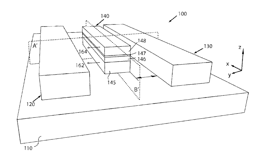
An electro-optical switch or router includes a semiconductor oxide substrate and first, second, and third semiconductor waveguides disposed on the semiconductor oxide substrate. The third waveguide includes a transparent conducting oxide layer, an oxide layer, a metal layer, and first and second electrodes coupled to the third waveguide. The electrodes are configured to bias and unbiased the third waveguide to effect optical switching in the electro-optical switch. The oxide layer is disposed between the transparent conducting oxide layer and the metal layer. The switch may further include a semiconductor layer disposed under the transparent conducting oxide layer between the transparent conducting oxide layer and the semiconductor oxide substrate. The first electrode may be coupled to the transparent conducting oxide layer, and the second electrode may be coupled to the metal layer.

What is claimed is:

1. An electro-optical switch comprising:

a low dielectric layer serving as a substrate;
a first high dielectric waveguide disposed on the low dielectric layer;
a second waveguide disposed on the low dielectric layer; and

a third waveguide disposed on the low dielectric layer, the third waveguide comprising:

a transparent conducting oxide layer;
a low dielectric layer;
a metal layer; and
a pair of electrodes coupled to the third waveguide and configured to bias the third waveguide to effect optical switching in the electro-optical switch.
2. The electro-optical switch of claim 1, wherein the low dielectric layer is disposed between the transparent conducting oxide layer and the metal layer.
3. The electro-optical switch of claim 1, wherein the transparent conducting oxide layer is formed from indium-tin-oxide and the metal layer is formed from aluminum or any low-resistive metal.
4. The electro-optical switch of claim 1, wherein the first waveguide is separated from the third waveguide by a first gap having a first width, and the second waveguide is separated from the third waveguide by a second gap having a second width.
5. The electro-optical switch of claim 4, wherein the first and second widths are equal.
6. The electro-optical switch of claim 1, wherein the first waveguide comprising an input for receiving light and an output for outputting light when the electro-optical switch is in a cross state, and wherein the second waveguide comprises an output for outputting the light received at the input when the electro-optical switch is in a bar state.
7. The electro-optical switch of claim 6, wherein for a light signal input having a wavelength from 1.30 to 1.85 micrometer, a ratio of coupling length of the electro-optical switch in the bar state to a coupling length of the electro-optical switch in the cross state is 35 and greater for a 400 nm bandwidth.
8. The electro-optical switch of claim 6, wherein an extinction ratio between the output of the first waveguide and the output of the second waveguide in the cross state is 21 dB and 7.3 dB in the bar state when the light has a 1.55 μm wavelength.
9. The electro-optical switch of claim 6, wherein an insertion loss in the cross state is about 1.5 dB.
10. The electro-optical switch of claim 6, wherein an energy per bit is about 9.0 fJ.
11. The electro-optical switch of claim 1, wherein the third waveguide further comprises a semiconductor layer disposed between the substrate and the transparent conducting oxide layer.

12. A method for coupling a light signal between the first, second, and third waveguides, the method comprising steps of:

providing a first waveguide configured to carry an optical signal;
providing a second waveguide configured to receive the optical signal from the first waveguide;
providing a third waveguide positioned at least partially between the first waveguide and the second waveguide, wherein the third waveguide has a transparent conducting oxide layer, low dielectric layer, and metal layer; and
selectively transferring by the third waveguide, the optical signal from said first waveguide to said second waveguide.
13. The method of claim 12, wherein the step of selectively comprises coupling a pair of electrodes to the third waveguide and controlling the pair of electrodes to bias the third waveguide to effect optical switching.

14. The method of claim 12, further comprising optimizing coupling between the first, second and third waveguides by:

performing an eigenmode analysis at a cross-section through the first, second, and third waveguides;
determining an optimized coupling length for a cross state of the electro-optical switch;
analyzing an effect of changing a width of a first gap between the first and third waveguides and a width of a second gap between the second and third waveguides to select an optimal value for the width of the first gap and an optimal value for the width of the second gap;
analyzing an effect of changing a width of the third waveguide and a height of the low dielectric layer to select an optimal value for the width of the third waveguide and an optimal value for the height of the low dielectric layer; and
calculating an extinction ratio between an output port of the first waveguide and an output port of the second waveguide for the electro-optical switch having optimal values for the width of the first gap, the width of the second gap, the width of the third waveguide, and the height of the low dielectric layer.
15. The method of claim 14, wherein the step of determining comprises a step of calculating a height of the low dielectric layer of the third waveguide.

16. The method of claim 14, wherein the step of determining comprises steps of:

calculating a height of the low dielectric layer of the third waveguide by matching an index of an anti-symmetric TM-polarized mode with one half of a difference between indices of first and second symmetric TM-polarized modes; and
calculating the optimized coupling length for the cross state of the electro-optical switch based on a bias-changed effective mode index between the first and second symmetric TM-polarized modes inside the third waveguide based on an operating wavelength.
17. The method of claim 14, further comprising a step of analyzing an effect on coupling by varying a thickness of the transparent conducting oxide layer.

18. A light routing switch comprising:

a first waveguide configured to carry an optical signal;
a second waveguide configured to receive the optical signal from said first waveguide; and,
a third waveguide positioned at least partially between said first waveguide and said second waveguide, said third waveguide selectively transferring the optical signal from said first waveguide to said second waveguide, wherein said third waveguide comprises a first layer of metal, a second layer of an oxide, a third layer of a transparent conductive oxide, and a fourth layer of a high dielectric, with an alternative design option that is similar the aforementioned one, but is comprised with an added second oxide between the transparent conductive oxide, and the high-dielectric underneath.
19. The router of claim 18, wherein said first, second and third waveguides are elongated and are arranged substantially parallel to each other.

20. An electro-optical switch comprising:

a low dielectric layer serving as a substrate;
a first high dielectric waveguide disposed on the low dielectric layer;
a second waveguide disposed on the low dielectric layer; and

a third waveguide disposed on the first low dielectric layer, the third waveguide comprising:

a transparent conducting oxide layer;
a low dielectric layer;
a metal layer; and
switching means controlling the effective modal index of the third waveguide via an electrical bias to the metal and TCO or alternatively, to the metal and bottom low-dielectric in the third waveguide to effect optical routing.

Share

Title

Silicon-based, broadband, waveguide-integrated electro-optical switch

Inventor(s)

Volker J. Sorger, Chenran Ye, Ke Liu

Assignee(s)

George Washington University

Publication #

9529158

Publication Date

December 27, 2016

Inquire about this intellectual property

Learn more about "A Breakthrough in Optical Switching: Revolutionizing Speed, Bandwidth, and Integration"