Advanced Nano Solar Cells for Peak Efficiency

Introduction

Imagine a solar cell engineered to capture sunlight more efficiently, converting it into energy with unmatched precision. This technology, based on donor and acceptor nanoparticulate conjugates within conductive polymer blends, is a breakthrough in the renewable energy field. By blending nanoparticles with conductive polymers, these photovoltaic cells offer a lightweight, flexible, and highly efficient solution for today’s energy demands.

This advanced cell design leverages the unique properties of nanoparticles to create a finely-tuned energy-harvesting surface. The donor and acceptor materials work together to capture and channel solar energy more effectively, achieving a level of efficiency that is difficult for traditional cells to match. Additionally, the use of conductive polymers makes these cells adaptable to a range of surfaces, enabling applications beyond the typical rigid solar panel. These cells can be integrated into building materials, wearable technology, or even used in portable solar products.

For manufacturers and developers in the renewable energy sector, this technology opens the door to innovative applications. Imagine creating solar solutions that are both visually appealing and power-efficient, appealing to eco-conscious consumers and forward-thinking businesses. With the growing focus on sustainability and energy independence, the potential market is vast.

Licensing this technology gives your business access to a unique, high-performance solar solution that differentiates you from competitors in the renewable energy field. Partnering with this technology means not only adopting a green, clean-energy approach but also investing in a solution that meets the increasing demands for flexible, efficient energy sources.
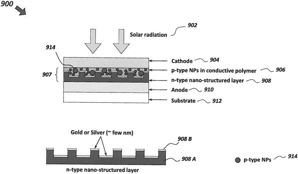
A photovoltaic cell includes a substrate layer, an anode layer on the substrate layer, an active layer on the anode layer, and a cathode layer on the active layer, wherein the active layer comprises a plurality of disparately sized n-type and p-type nano-particles of different semiconductor materials randomly distributed in a conductive polymer blend. The n-type nano-particles can include either ZnO or In2O3 nano-particles, and the p-type nano-particles can include either NiO or La2O3 nano-particles. The conductive polymer blend can include P3HT. The bandgaps of the nano-particles have corresponding energies ranging from the near ultraviolet to the far infrared.

The invention claimed is:

1. A photovoltaic cell, comprising:

a substrate layer;
an anode layer on the substrate layer;
an n-type nano-structured layer on the anode layer;
an active layer on the n-type nano-structured layer; and
a cathode layer on the active layer
wherein the active layer comprises a plurality of disparately sized p-type nano-particles,
wherein junctions randomly form between the n-type nano-structured layer and the disparately sized p-type nano-particles;
wherein the n-type nano-structured layer comprises nano-structure rectangular ridges on the n-type nano-structured layer extending into the active layer, the ridges each having a face region facing the cathode and side regions facing adjacent ridges, and the n-type nano-structured layer having valley regions between the ridges; and
further comprising gold or silver on the n-type nano-structured layer, the gold or silver being located on the face regions of the nano-structure rectangular ridges and in the valley regions of the n-type nano-structured layer, but not on the side regions of the nano-structure rectangular ridges, wherein the junctions randomly form between the side regions of the nano-structure rectangular ridges and the disparately sized p-type nano-particles.
2. The photovoltaic cell of claim 1, wherein n-type nano-particles comprise either ZnO or In2O3 nano-particles.
3. The photovoltaic cell of claim 1, wherein the p-type nano-particles comprise either NiO or La2O3 nano-particles.
4. The photovoltaic cell of claim 1, wherein the active layer further comprises a first conductive polymer comprising poly(3-hexyl)thiophene (P3HT).

5. The photovoltaic cell of claim 1, wherein:

bandgaps of the n-type and p-type nano-particles both have corresponding energies ranging from the near ultraviolet to the far infrared.
6. The photovoltaic cell of claim 1, wherein the photovoltaic cell is flexible.
7. The photovoltaic cell of claim 1, wherein the substrate layer comprises a flexible layer.
8. The photovoltaic cell of claim 1, wherein the anode layer comprises indium tin oxide (ITO).
9. The photovoltaic cell of claim 1, wherein the cathode layer comprises gold or aluminum.
10. The photovoltaic cell of claim 1, wherein the active layer further comprises gold or silver nano-particles.
11. The photovoltaic cell of claim 1, wherein the active layer comprises a plurality of disparately sized n-type nano-particles.
12. The photovoltaic cell of claim 1, wherein the n-type nano-structured layer consists of a single material, and wherein the rectangular ridges have widths and heights equal to or less than the electron and hole mobility of the material.
13. The photovoltaic cell of claim 1, wherein the active layer further comprises gold or silver nano-particles.

14. A method of manufacturing a photovoltaic cell, the method comprising:

providing a substrate layer;
forming an anode layer on the substrate layer;
forming an n-type nano-structured layer on the anode layer;
forming an active layer on the n-type nano-structured layer; and
forming a cathode layer on the active layer,
wherein the active layer comprises a plurality of disparately sized p-type nano-particles randomly distributed in a first conductive polymer,
wherein junctions randomly form between the n-type nano-structured layer and the disparately sized p-type nano-particles;
wherein the n-type nano-structured layer comprises nano-structure rectangular ridges on the n-type nano-structured layer extending into the active layer, the ridges each having a face region facing the cathode and side regions facing adjacent ridges, and the n-type nano-structured layer having valley regions between the ridges; and
further comprising forming gold or silver on the n-type nano-structured layer, the gold or silver being located on the face regions of the nano-structure rectangular ridges and in the valley regions of the n-type nano-structured layer, but not on the side regions of the nano-structure rectangular ridges, wherein the junctions randomly form between the side regions of the nano-structure rectangular ridges and the disparately sized p-type nano-particles.
15. The method of claim 14, wherein the active layer further comprises a plurality of disparately sized n-type nano-particles.
16. The method of claim 14, wherein the active layer further comprises gold or silver nano-particles.
17. The photovoltaic cell of claim 1, further comprising a first interfacial layer interposed between the active layer and the cathode layer.
18. The photovoltaic cell of claim 17, further comprising a plurality of gold nano-particles in a conductive polymer of the interfacial layer.
19. The method of claim 14, further comprising forming a first interfacial layer between the active layer and the cathode layer.
20. The method of claim 14, wherein the interfacial layer comprises a plurality of gold nano-particles in a conductive polymer of the interfacial layer.

Share

Title

Photovoltaic cells based on donor and acceptor nano-particulate conjugates in conductive polymer blends

Inventor(s)

Naga Korivi, Kalyan Das

Assignee(s)

Tuskegee University

Patent #

11374188

Patent Date

June 28, 2022

Inquire about this intellectual property

Learn more about "Advanced Nano Solar Cells for Peak Efficiency"