Boost Data Transfer Efficiency with Hybrid Photonic-Plasmonic Interconnects

Introduction

As global data demands soar, the need for faster, more efficient interconnect technologies has become critical for data centers, semiconductor manufacturers, and telecommunications providers. Traditional electronic interconnects are approaching their physical limits, unable to meet the speed, bandwidth, and energy efficiency requirements of modern communication systems. Our Hybrid Photonic Plasmonic Interconnects (HyPPI) technology provides a breakthrough solution, combining the best of photonic and plasmonic systems to deliver unmatched performance in data transmission.

The Problem

Conventional interconnect technologies, based purely on electronics or photonics, face significant limitations. Electronic interconnects, while effective, are slow and power-hungry when scaled to meet the demands of high-speed data transmission. On the other hand, photonic systems, while faster, often suffer from inefficiencies when trying to bridge the gap between optical and electronic domains. This has led to bottlenecks in data centers, cloud computing infrastructure, and high-speed telecommunications networks, which are increasingly strained by the global demand for more data at faster speeds.

The Solution

Our HyPPI technology seamlessly integrates photonic and plasmonic systems, leveraging the speed of light and the compactness of plasmonic waves to create an interconnect that performs well beyond the capabilities of traditional methods. With both intrinsic and extrinsic modulation options, HyPPI offers unparalleled flexibility, enabling precise control over data transfer rates while minimizing energy consumption.

Key Benefits

  1. Superior Data Transmission: The hybrid approach allows for incredibly fast data transfer speeds while maintaining low latency, making it ideal for large-scale data centers, high-performance computing environments, and advanced telecommunication networks.
  2. Energy Efficiency: Traditional interconnects often require substantial energy to function at high speeds. Our hybrid system significantly reduces power consumption, cutting operational costs and improving sustainability, which is increasingly critical for modern data-driven industries.
  3. Flexible Modulation Options: The integration of both intrinsic and extrinsic modulation provides enhanced control over how data is transferred, allowing for greater adaptability to different systems and needs. This flexibility is a major advantage when designing next-generation chips or communication systems.
  4. Scalability: Whether you’re developing components for cutting-edge telecommunications or next-generation data centers, this technology is scalable to fit a variety of needs, from smaller consumer electronics to large-scale industrial applications.

Why License This Technology?

Licensing HyPPI offers your company a direct path to improving data transmission efficiency and performance in a rapidly evolving technological landscape. The hybrid approach, combining the best aspects of photonic and plasmonic systems, allows you to deliver products that not only meet today’s data demands but are ready for the future. It’s a strategic advantage for industries that rely on high-speed communication and data transfer.

Conclusion

As data demands continue to rise, the need for efficient, scalable interconnect technologies is critical. By licensing this hybrid photonic-plasmonic interconnect technology, you position your company at the forefront of the next wave of high-speed data communication, ensuring that your products deliver the speed, flexibility, and efficiency the market demands.
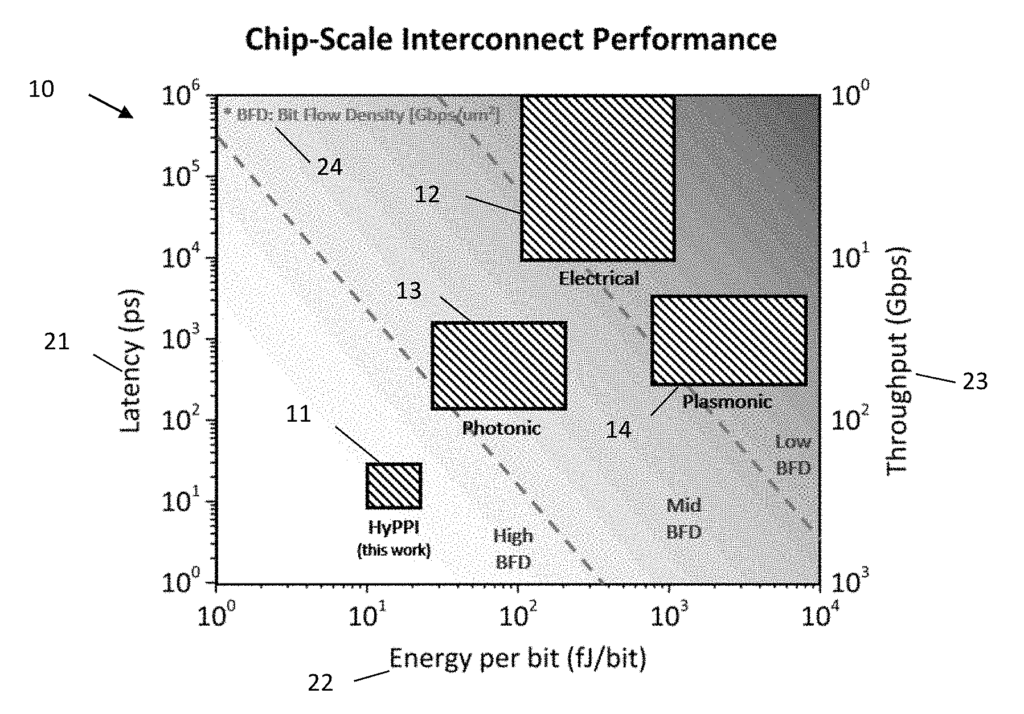
The Hybrid Photonic Plasmonic Interconnect (HyPPI) combines both low loss photonic signal propagation and passive routing with ultra-compact plasmonic devices. These optical interconnects therefore uniquely combine fast operational data-bandwidths (in hundreds of Gbps) for light manipulation with low optical attenuation losses by hybridizing low loss photonics with strong light-matter-interaction plasmonics to create, modulate, switch and detect light efficiently at the same time. Initial implementations were considered for on-chip photonic integration, but also promising for free space or fiber-based systems. In general two technical options exist, which distinguished by the method the electric-optic conversion is executed: the extrinsic modulation method consists of an continuous wave source such as an LED or laser operating at steady power output, and signal encoding is done via an electro-optic modulator downstream of the source in the interconnect. In contrast, in the intrinsic method, the optical source is directly amplitude modulated.

The invention claimed is:

1. An intrinsic hybrid photonic plasmonic system, comprising:

a plasmonic laser configured to generate an optical signal;
a photonic waveguide configured to propagate the optical signal; and
a plasmonic detector configured to detect the optical signal.
2. The system of claim 1, wherein said photonic waveguide is diffraction-limited.
3. The system of claim 1, further comprising an electronic driver configured to turn said plasmonic laser ON and OFF to modulate the optical signal from said plasmonic laser to load electronic data to provide a modulated optical signal, and said plasmonic detector is configured to detect the modulated optical signal.
4. The system of claim 1, further comprising a plasmonic laser configured to provide the optical signal and to turn ON and OFF to add electronic data to the optical signal to provide a modulated optical signal, and said photonic detector is configured to detect the modulated optical signal.
5. The system of claim 1, wherein the optical signal has a wavelength of 1550 nm.
6. The system of claim 1, wherein the optical signal has a wavelength and said waveguide is near-transparent for the wavelength.
7. The system of claim 6, wherein the waveguide is low loss for the wavelength.
8. The system of claim 1, wherein the total energy cost includes the laser pumping energy, the electrical laser driver energy and the photodetector bias energy and the laser pumping energy compensates all the channel losses.
9. The system of claim 8, wherein the channel losses include waveguide loss, laser efficiency, crosstalk and photodetector responsivity.
10. The system of claim 1, said system having a point-to-point latency is less than 100 ps/cm, an energy per bit is about or below 15 fJ/bit, a transmission loss less than 1.1 dB/cm, a bit flow density of 0.01˜1 Gbps/μm2, and a cross-section of 2 μm2.
11. An extrinsic hybrid photonic plasmonic system, comprising:

a plasmonic laser configured to generate light;
a photonic waveguide configured to propagate an optical signal; and
a plasmonic modulator configured to manipulate the optical signal to load electronic data into the optical signal, to provide a modulated optical signal; and
a plasmonic detector configured to detect the modulated optical signal.
12. The system of claim 11, further comprising a plasmonic laser configured to provide the optical signal to said photonic waveguide.
13. The system of claim 11, further comprising a photonic modulated signal waveguide configured to propagate the modulated optical signal from said plasmonic modulator to said plasmonic detector with plasmonic-photonic coupler.
14. The system of claim 11, wherein the optical signal has a wavelength of 1550 nm.
15. The system of claim 11, wherein the optical signal has a wavelength and said waveguide is near-transparent (low loss) for the wavelength.
16. The system of claim 11, wherein the total energy cost includes the laser pumping energy, the electrical modulator driver energy, the modulator energy, and the photodetector bias energy and the laser pumping energy compensates all the channel losses, which includes waveguide loss, coupler loss, laser efficiency, crosstalk and photodetector responsivity.
17. The system of claim 11, said system having a point-to-point latency is less than 100 ps/cm, an energy per bit is about or below 25 fJ/bit, a transmission loss less than 2.1 dB/cm, a bit flow density of 0.01˜1 Gbps/μm2, and a cross-section of 2 μm2.
18. A method for calculating a laser power for photonic, plasmonic and hybrid photonic plasmonic data interconnect systems having a laser, photodetector and a link comprising a waveguide, the method comprising:

providing the minimum current that is required by a next stage to which the link is connected;
determining at the photodetector, a minimum light power that is required by the photodetector to generate the minimum current;
determining at the laser, a minimum laser output power to compensate a channel loss of the waveguide, modulator, coupler and waveguide crosstalk losses; and
determining at the laser, the laser power based on laser efficiency.
19. The method of claim 18, further comprising predicting at the processing device, a laser energy efficiency in the unit of J/bit based on different cavities of the laser and coding schemes for the intrinsic system of claim 1.
20. The method of claim 19, wherein different laser cavities give laser different power efficiency at under different scaling and the coding schemes affect the coding efficiency, which further affect the energy that a laser needs to send a bit of data.
21. The method of claim 18, further comprising predicting at the processing device, a required laser energy for different device cavities and photonic waveguides for the extrinsic system of claim 11.
22. A method for predicting the capacity of an entire channel of a waveguide, the method comprising:

calculating a maximum bandwidth of the channel in hertz based on a lowest bandwidth device on the channel; and
calculating a channel capacity of the channel in bits per second by using the maximum bandwidth and a signal-to-noise ratio (SNR) of the channel, wherein the channel capacity equals to bandwidth×log 2(1+SNR).
23. The method of claim 22, wherein a minimum capacity of the channel is equal to the maximum bandwidth of the channel when the signal-to-noise ratio equals to 1, which equals to a worst case.
24. A method of benchmarking interconnect performance with on-chip footprint, namely bit flow density (BFD), which is a number of bits transmitted through a certain chip width (cross-section) to reach a specific required communication length, which is highly related to a size of each device and spacing, the method comprising:

simulating on a processing device, a propagation speed and length for different waveguide sizes;
simulating on the processing device, a crosstalk leakage among waveguides under different spacing;
calculating for a specific chip length, a number of signal repeaters that a channel needs to reach the chip length based on a propagation length;
calculating for a specific chip width, a number of channels that can stack into the chip width based on the device footprint and spacing; and
calculating an overall bit flow density by using a total capacity of all the channels divided by the specific chip area which is the chip length by the chip width.
25. The method of claim 24, wherein the chip length is a first side of a chip area and the chip width is a second side of the chip area opposite the first side.

Share

Title

Hybrid photonic plasmonic interconnects (HyPPI) with intrinsic and extrinsic modulation options

Inventor(s)

Shuai Sun, Volker J. Sorger, Tarek El-Ghazawi, Vikram K. NARAYANA, Abdel-Hameed A. BADAWY

Assignee(s)

George Washington University

Patent #

10256600

Patent Date

April 9, 2019

Inquire about this intellectual property

Learn more about "Boost Data Transfer Efficiency with Hybrid Photonic-Plasmonic Interconnects"