Harnessing the Power of Surface Acoustic Waves for Advanced Semiconductor Applications

Introduction

In today’s rapidly evolving technological landscape, the demand for faster, smaller, and more efficient electronic components continues to grow. Surface acoustic wave (SAW) technology offers a unique solution for a range of applications, from telecommunications to quantum computing. Our innovative method for generating and enhancing surface acoustic waves on highly doped p-type III-V semiconductor substrates unlocks new possibilities for high-performance electronics and devices.

The Challenge

Current surface acoustic wave technologies, while effective, are often limited by the materials they rely on, particularly in high-frequency applications. Traditional semiconductor substrates can struggle to meet the demands of modern devices that require both high-speed signal processing and precision. As a result, industries like telecommunications and advanced sensing are in need of a more efficient, scalable solution for generating surface acoustic waves.

The Solution

Our patented approach utilizes highly doped p-type III-V semiconductor substrates to generate and enhance surface acoustic waves, significantly improving performance and reliability. This method not only increases the efficiency of surface wave generation but also provides enhanced control over wave propagation, leading to improved signal processing capabilities. Whether for use in RF filters, sensors, or other semiconductor devices, this technology offers a pathway to enhanced performance and smaller, more efficient components.

Key Benefits

  1. High-Speed Signal Processing: By enhancing the generation of surface acoustic waves, this technology enables faster, more efficient signal processing. It’s ideal for applications in telecommunications, where high-frequency RF filters are essential for modern wireless communication systems.
  2. Improved Device Performance: The use of highly doped III-V semiconductor substrates leads to enhanced control over wave propagation, resulting in more accurate and reliable devices. This is especially beneficial for sensors, oscillators, and other components that require precise signal processing.
  3. Versatile Applications: From advanced acoustic sensors and RF filters to potential uses in quantum computing, this technology offers versatility across multiple industries. Its ability to integrate with existing semiconductor manufacturing processes makes it scalable for a wide range of applications.

Why License This Technology?

Licensing this advanced SAW technology positions your company at the forefront of semiconductor innovation. With its potential to improve performance in telecommunications, electronics, and beyond, this solution offers a unique advantage in developing the next generation of high-performance devices.
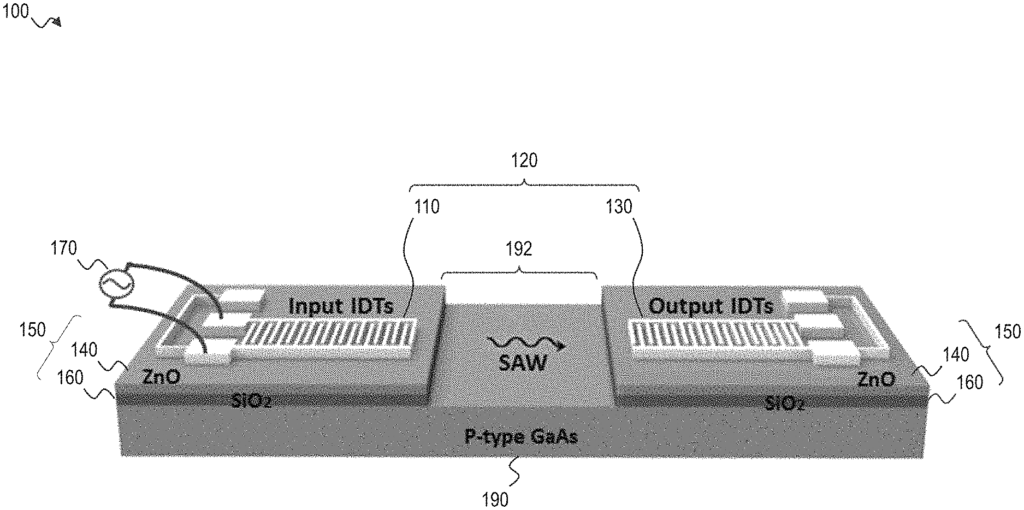
A device employing the generation and enhancement of surface acoustic waves on a highly doped p-type III-V semiconductor substrate (e.g., GaAs, GaSb, InAs, or InGaAs). The device includes two SiO2/ZnO islands, each including a SiO2 buffer layer deposited on the doped p-type III-V semiconductor substrate and a ZnO layer deposited on the SiO2 buffer layer. An input interdigital transducers (IDT) and an output IDT are each patterned on one of the SiO2/ZnO islands. The IDTs generates surface acoustic waves along an exposed surface of the highly doped p-type III-V semiconductor substrate. The surface acoustic waves improve the photoelectric and photovoltaic properties of the device. The device is manufactured using a disclosed technique for propagating strong surface acoustic waves on weak piezoelectric materials. Also disclosed is a photodetector developed using that technique.
What is claimed is:

1. A device, comprising:

a doped p-type III-V semiconductor substrate;
two silicon dioxide (SiO2) and zinc oxide (ZnO) islands, each of the SiO2/ZnO islands comprising a SiO2 buffer layer deposited on the doped p-type III-V semiconductor substrate and a ZnO layer deposited on the SiO2 buffer layer;
two interdigital transducers (IDTs) each patterned on one of the SiO2/ZnO islands; and
an exposed surface of the doped p-type III-V semiconductor substrate between the two SiO2/ZnO islands.
2. The device of claim 1, wherein:

the IDTs include an input IDT that generates surface acoustic waves and an output IDT that receives the surface acoustic waves.
3. The device of claim 2, wherein the input IDT generates surface acoustic waves along the exposed surface of the doped p-type III-V semiconductor substrate.
4. The device of claim 3, wherein:

the doped p-type III-V semiconductor substrate has a (100) surface and a [011] direction; and
the input IDT generates surface acoustic waves along the [011] direction of the doped p-type III-V semiconductor substrate.
5. The device of claim 1, wherein the SiO2 buffer layer of each SiO2/ZnO island has a thickness of at least 800 nanometers.
6. The device of claim 1, wherein the doped p-type III-V semiconductor substrate is gallium arsenide.
7. The device of claim 1, wherein the doped p-type III-V semiconductor substrate is gallium antimonide, indium arsenide, or indium gallium arsenide.
8. A method of making a device, the method comprising:

depositing a silicon dioxide (SiO2) buffer layer on a doped p-type III-V semiconductor substrate;
depositing a zinc oxide (ZnO) layer on the SiO2 buffer layer;
patterning two interdigital transducers (IDTs) on the ZnO layer; and
etching a portion of the ZnO layer and the SiO2 buffer layer between the two IDTs to form two ZnO/SiO2 islands, each supporting one of the two IDTs, and an exposed surface of the doped p-type III-V semiconductor substrate between the two IDTs.
9. The method of claim 8, wherein:

the IDTs include an input IDT that generates surface acoustic waves and an output IDT that receives the surface acoustic waves.
10. The method of claim 9, wherein the input IDT is patterned such that it generates surface acoustic waves along the exposed surface of the doped p-type III-V semiconductor substrate.
11. The method of claim 10, wherein:

the doped p-type III-V semiconductor substrate has a (100) surface and a [011] direction; and
the input IDT is patterned such that it generates surface acoustic waves along the [011] direction of the doped p-type III-V semiconductor substrate.
12. The method of claim 8, wherein the SiO2 buffer layer is deposited such that it has a thickness of at least 800 nanometers.
13. The method of claim 8, wherein the doped p-type III-V semiconductor substrate is gallium arsenide.
14. The method of claim 8, wherein the doped p-type III-V semiconductor substrate is gallium antimonide, indium arsenide, or indium gallium arsenide.
15. A photodetector, comprising:

a III-V semiconductor substrate;
a silicon dioxide (SiO2) buffer layer deposited on the doped p-type III-V semiconductor substrate;
a two-dimensional (2D) material comprising a single layer of atoms on the III-V semiconductor substrate;
two zinc oxide (ZnO) islands deposited on the SiO2 buffer layer on either side of the 2D material;
two interdigital transducers (IDTs) patterned on each of the two ZnO islands, the two IDTs including an input IDT that generates surface acoustic waves and an output IDT that receives the surface acoustic waves,
a source electrode;
a drain electrode; and
a gate electrode.
16. The photodetector of claim 15, wherein the input IDT generates surface acoustic waves along the surface of the 2D material.
17. The photodetector of claim 15, wherein a current between the source electrode and the drain electrode varies in response to visible or infrared light that is incident to the 2D material.
18. The photodetector of claim 15, wherein transmission characteristics of the surface acoustic waves vary in response to visible or infrared light that is incident to the 2D material.
19. The photodetector of claim 15, wherein the III-V semiconductor substrate is gallium antimonide.
20. The photodetector of claim 15, wherein the doped p-type III-V semiconductor substrate is gallium arsenide, indium arsenide, or indium gallium arsenide.
21. A device, comprising:

a doped p-type III-V semiconductor substrate with a crystalline surface;
a piezoelectric coupling layer that increases the intensity of surface acoustic waves on the doped p-type III-V semiconductor substrate;
a buffer layer, deposited on the doped p-type III-V semiconductor substrate below the piezoelectric coupling layer, that masks the crystalline surface of the doped p-type III-V semiconductor substrate and increases the piezoelectricity of the piezoelectric coupling layer;
two interdigital transducers (IDTs), each patterned on piezoelectric coupling layer and the buffer layer, that increases the intensity of surface acoustic waves on the doped p-type III-V semiconductor substrate;
an exposed surface of the doped p-type III-V semiconductor substrate, between the two IDTs.

Share

Title

Generation and enhancement of surface acoustic waves on a highly doped p-type III-V semiconductor substrate

Inventor(s)

Boqun Dong, Mona Zaghloul

Assignee(s)

George Washington University

Patent #

11211913

Patent Date

December 28, 2021

Inquire about this intellectual property

Learn more about "Harnessing the Power of Surface Acoustic Waves for Advanced Semiconductor Applications"