Next-Level Optical Modulation for High-Speed Data and Photonic Systems

Introduction

In the age of high-speed data and advanced communication networks, the demand for faster, more efficient optical modulation technologies has never been greater. As industries move toward photonic systems that can outpace traditional electronics, the ability to modulate light quickly and with precision is critical for driving new advancements in telecommunications, data centers, and quantum computing. Our patented electro-refractive modulation technology in photonic structures offers a breakthrough solution for industries seeking to expand the capabilities of their optical communication systems.

Current Barriers in Optical Modulation Technologies

Traditional methods of optical modulation often face performance bottlenecks, especially when it comes to achieving the speeds necessary for next-generation data transmission and processing. Many existing technologies rely on electro-optic or thermo-optic effects, which can be limited by slower response times, higher power consumption, or complex integration processes. In a world where data demands are growing exponentially, these limitations hinder the development of more scalable and efficient photonic systems.

Telecommunications providers and data centers, in particular, require optical modulators that can handle massive amounts of data traffic without compromising on speed, efficiency, or performance. The need for more compact, energy-efficient, and faster optical modulators has become a key area of focus in the industry.

Electro-Refractive Modulation: A Superior Approach

Our electro-refractive modulation technology is designed to overcome these challenges by providing a highly efficient and fast method for modulating light within photonic structures. The innovation leverages the electro-refractive effect—where the refractive index of a material is altered by an applied electric field—to achieve precise and rapid modulation. This allows for enhanced data transmission speeds, reduced power consumption, and greater overall efficiency in optical systems.

This technology is particularly well-suited for telecommunications networks, where high-speed data transmission is critical, as well as in quantum computing, where light manipulation plays a key role in information processing. Additionally, the electro-refractive modulation can be seamlessly integrated into existing photonic circuits, making it a flexible solution for manufacturers looking to upgrade their systems without overhauling their infrastructure.

Key Advantages

  • High-Speed Data Transmission: By utilizing electro-refractive effects, this technology enables faster data modulation, ideal for next-generation telecommunication networks.
  • Lower Power Consumption: The efficiency of this method reduces the power required for optical modulation, making it suitable for energy-conscious applications.
  • Scalable and Flexible: The technology can be easily integrated into existing photonic devices and circuits, offering flexibility in both design and application.
  • Versatile Applications: From telecommunications to quantum computing, the broad range of uses makes this a valuable asset for industries seeking to enhance their photonic systems.

A Critical Asset for the Future of Photonics

Licensing this electro-refractive modulation technology provides businesses with a cutting-edge tool to lead in the photonics and telecommunications sectors. With its ability to deliver faster, more efficient data transmission and processing, this technology is poised to become an essential component in the future of high-speed communication and photonic-based computing systems.
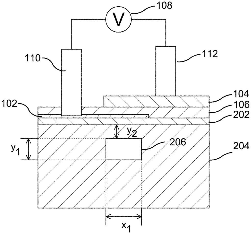
Methods, systems, and devices are described for electro-optic tuning. An example device may comprise a first layer comprising a transition metal di-chalcogenide material, a second layer comprising a conductive material, and a third layer comprising a dielectric material. The third layer may be disposed at least partially between the first layer and the second layer. An electrical potential difference applied between the first layer and the second layer may cause a tunable refractive index change in the first layer.

What is claimed:

1. A device configured for phase modulation, the device comprising:

a first layer comprising a monolayer transition metal di-chalcogenide material;
a second layer comprising a conductive material;
a third layer comprising a dielectric material and disposed at least partially between the first layer and the second layer, wherein an electrical potential difference applied between the first layer and the second layer causes a tunable refractive index change in the first layer; and
a waveguide disposed in a substrate such that the waveguide is separated from the first layer, wherein changes in the refractive index of the first layer cause phase modulation in a near-infrared range of light in the waveguide.
2. The device of claim 1, wherein the first layer is part of a component of one or more of an optical network, a phased array, or an optical delay line.
3. The device of claim 1, wherein the first layer, the second layer, and the third layer are disposed in one or more of a capacitor configuration or a parallel plate capacitor configuration.
4. The device of claim 1, wherein the transition metal di-chalcogenide material comprises one or more of tungsten, molybdenum, sulfur, or selenium.
5. The device of claim 1, wherein the transition metal di-chalcogenide material comprises one or more of WS2, WSe2, MoS2, or MoSe2.
6. The device of claim 1, wherein the third layer comprises hafnium oxide.
7. The device of claim 1, wherein the conductive material comprises indium tin oxide.
8. The device of claim 1, wherein the refractive index change is one or more of (i) greater than about 10 percent, (ii) in a range of about 5 percent to about 15 percent, or (iii) in a range of about 10 percent to about 15 percent.
9. The device of claim 1, wherein the waveguide is separated by from the first layer by an additional layer disposed in between the substrate the first layer.
10. The device of claim 1, wherein the device is engineered to optimize modal overlap with a photonic mode.
11. The device of claim 1, wherein the substrate is planarized.
12. The device of claim 1, wherein optical absorption of the device during phase modulation is minimized to less than 0.012 dB/cm/V.
13. A method comprising:

receiving a signal; and
causing, based on the signal, phase modulation in the near-infrared range of light in a waveguide based on modifying an electrical potential difference between a first layer and a second layer to cause a change in a refractive index in the first layer, wherein the first layer comprises a monolayer transition metal di-chalcogenide material and the second layer comprises a conductive material, and wherein a third layer comprising a dielectric material is disposed at least partially between the first layer and the second layer, and wherein the waveguide is disposed in a substrate such that the waveguide is separated from the first layer.
14. The method of claim 13, wherein the first layer is part of a component of one or more of an optical network, a phased array, or an optical delay line.
15. The method of claim 13, wherein the first layer, the second layer, and the third layer are disposed in one or more of a capacitor configuration or a parallel plate capacitor configuration.
16. The method of claim 13, wherein the transition metal di-chalcogenide material comprises one or more of WS2, WSe2, MoS2, or MoSe2.
17. The method of claim 13, wherein the change in the refractive index is one or more of (i) greater than about 10 percent, (ii) in a range of about 5 percent to about 15 percent, or (iii) in a range of about 10 percent to about 15 percent.
18. An electro-optical device, comprising:

a component comprising a first layer and a second layer, wherein the first layer comprises a monolayer transition metal di-chalcogenide material;
a waveguide disposed in a substrate such that the waveguide is separated from the first layer; and
a logic unit configured to cause phase modulation in the near-infrared range of light in the waveguide based on modifying an electrical potential difference between the first layer and the second layer to change a refractive index in one or more of the first layer or the second layer.

Share

Title

Electro-refractive modulation in photonic structures

Inventor(s)

Michal LipsonJames HoneNanfang YuIpshita DattaSanghoon ChaeGaurang R BhattDmitri N Basov

Assignee(s)

Columbia University in the City of New York

Patent #

11256112

Patent Date

February 22, 2022

Inquire about this intellectual property

Learn more about "Next-Level Optical Modulation for High-Speed Data and Photonic Systems"