Unlocking the Future of Material Science with Artificial Lattice Engineering
Introduction
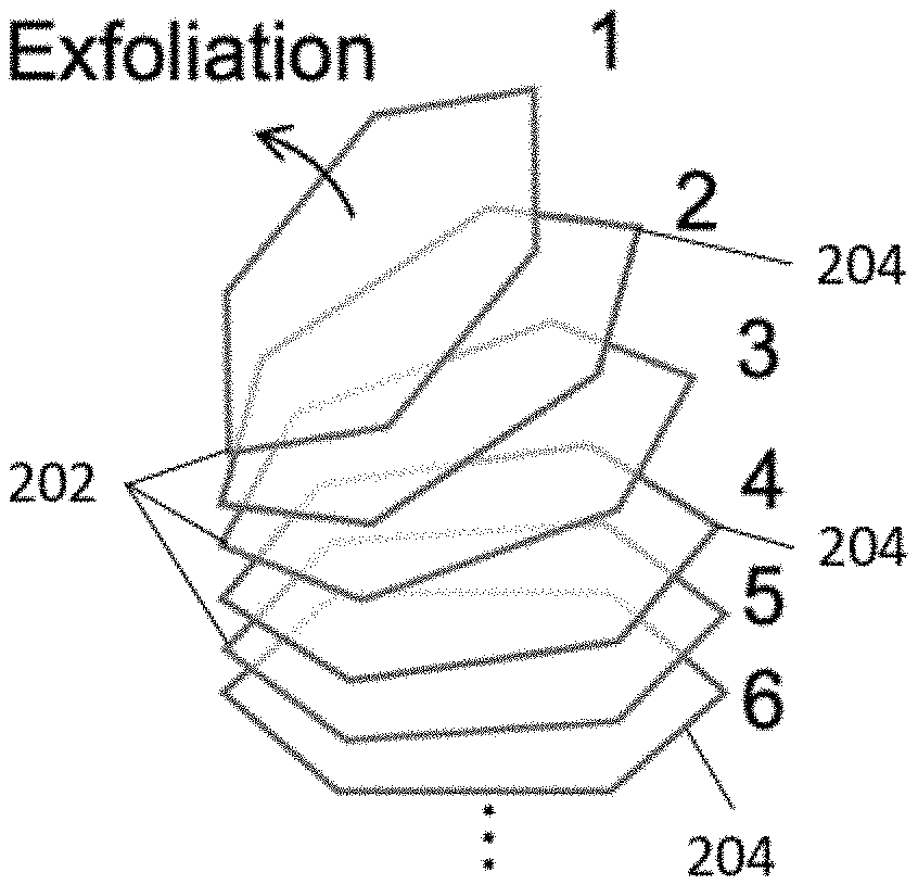
Two-dimensional (2D) materials, such as graphene and other Van der Waals crystals, are at the forefront of next-generation technologies. Their unique properties—extreme thinness, high electrical conductivity, and mechanical strength—make them highly sought after in industries ranging from electronics to quantum computing. However, one of the major barriers to fully exploiting their potential is the difficulty in manipulating these materials at the macroscopic scale. Our patented technology offers an innovative system for disassembling two-dimensional crystals into macroscopic monolayers and reassembling them into custom artificial lattices, enabling the precise control and use of these materials in advanced applications.
Limitations of Traditional Fabrication Techniques
Today’s techniques for working with 2D materials often fall short when it comes to scalability and precision. Methods for creating monolayers of Van der Waals crystals, while effective at the laboratory scale, struggle to meet the requirements for large-scale manufacturing. Furthermore, the ability to manipulate these materials into new lattice structures opens up possibilities for custom-engineered materials with entirely new properties. Unfortunately, existing tools don’t offer the level of control needed to unlock these advanced capabilities, limiting the practical applications of 2D materials in real-world devices.
A Novel Approach to 2D Material Engineering
Our patented system is designed to address these challenges by providing a method to disassemble two-dimensional Van der Waals crystals into macroscopic monolayers and reassemble them into custom artificial lattice structures. This breakthrough technology allows for the creation of entirely new materials with tailored electrical, thermal, and optical properties, expanding the use of 2D materials beyond their current applications.
The ability to create artificial lattices from reassembled 2D monolayers enables the design of materials that can be fine-tuned for specific functions. Whether for use in transistors with enhanced performance, sensors with unprecedented sensitivity, or quantum computing applications requiring precise lattice structures, this technology opens the door to a new era of material customization and innovation.
Key Advantages
- Scalable and Precise: The system allows for the manipulation of 2D materials at a macroscopic scale, making it feasible for large-scale manufacturing.
- Tailored Material Properties: By reassembling 2D crystals into artificial lattices, new materials can be engineered with specific, desired properties for specialized applications.
- Broad Industrial Application: From semiconductors to advanced optics and quantum computing, this technology offers vast potential across multiple high-tech sectors.
- Next-Level Innovation: It enables the creation of entirely new classes of materials that were previously unattainable, pushing the boundaries of what is possible in nanotechnology and material science.
An Opportunity to Lead in Advanced Material Manufacturing
Licensing this technology allows companies in the nanotechnology, electronics, and semiconductor industries to lead the charge in creating next-generation materials. By offering the ability to manipulate and customize 2D materials at scale, this system provides a competitive edge in the race to develop more efficient, powerful, and innovative devices.

- Abstract
- Claims
Share
Title
Systems and methods for disassembling two-dimensional van der waals crystals into macroscopic monolayers and reassembling into artificial lattices
Inventor(s)
James Hone, Fang Liu, Xiaoyang Zhu, Sang Hoon Chae
Assignee(s)
Columbia University in the City of New York
Patent #
20210172087
Patent Date
June 10, 2021
