Efficient Electronics with Direct Graphene Synthesis

Introduction

Graphene is one of the most promising materials in modern science, known for its exceptional electrical, thermal, and mechanical properties. However, one of the biggest challenges in leveraging graphene’s potential lies in the complexity of synthesizing high-quality graphene films on various substrates. Our patented method for the direct synthesis of reduced graphene oxide (rGO) films on dielectric substrates offers a highly efficient and scalable solution. This technology brings graphene closer to large-scale applications in electronics, nanotechnology, and semiconductor industries, offering a new path for developing high-performance devices.

Barriers in Traditional Graphene Synthesis

While graphene’s potential in electronics and nanotechnology is immense, traditional methods of producing graphene or reduced graphene oxide films are often cumbersome and inefficient. These processes frequently involve multiple steps, requiring transfer from one substrate to another, which increases the risk of defects, contamination, and performance degradation. The inability to directly synthesize graphene films on key substrates such as dielectrics limits the material’s application in next-generation devices, including transistors, sensors, and flexible electronics.

In industries where precision, scalability, and material performance are critical, there is a growing need for simpler, more reliable methods to integrate graphene films directly onto dielectric substrates without compromising quality or functionality.

Direct Synthesis for Seamless Integration

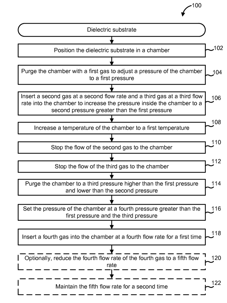
Our patented method provides a direct synthesis approach, allowing for the formation of reduced graphene oxide films directly on dielectric substrates. This method streamlines the process by eliminating the need for transfer steps, reducing potential defects, and maintaining the structural integrity of the graphene oxide during reduction. The resulting films are of high quality, with enhanced electrical conductivity and thermal properties, making them ideal for applications in electronic devices, flexible electronics, and nanoelectronics.

This direct synthesis approach is not only more efficient but also scalable, enabling the production of high-performance graphene-based materials for a wide range of industrial applications. Whether in developing high-speed transistors, sensors, or advanced circuit components, this technology offers a more seamless integration of graphene into existing manufacturing processes, unlocking new possibilities in the electronics and nanotechnology sectors.

Key Benefits

  • Direct Integration: Synthesize reduced graphene oxide films directly on dielectric substrates, eliminating transfer steps and reducing defects.
  • Improved Material Performance: Enhanced electrical and thermal properties of the rGO films make them suitable for high-performance electronic applications.
  • Scalable Process: Ideal for large-scale production in industries such as semiconductors, electronics, and nanotechnology.
  • Versatile Applications: Suitable for use in transistors, sensors, nanoelectronics, and flexible electronic devices.

Enhance Electronic Devices with Directly Synthesized Graphene Films

Licensing this direct synthesis technology provides companies in electronics, nanotechnology, and materials science with an advanced solution for integrating graphene into next-generation devices. With its ability to streamline the production process while delivering high-quality films, this technology offers a powerful tool for developing more efficient, scalable, and high-performance electronic components.

A method for coating a dielectric substrate with a R-GO film includes positioning the dielectric substrate in a chamber which is purged with a first gas to adjust a pressure of the chamber to a first pressure. A second gas at a second flow rate and a third gas at a third flow rate is inserted into the chamber to increase the chamber pressure to a second pressure greater than the first pressure. A chamber temperature is increased to a first temperature. The flow of the second gas and the third gas is stopped. The chamber is purged to a third pressure higher than the first pressure and lower than the second pressure. The pressure of the chamber is set at a fourth pressure greater than the first pressure and the third pressure. A fourth gas is inserted into the chamber at a fourth flow rate for a first time.

What is claimed is:

1. A method for coating a dielectric substrate with a reduced graphene oxide film, comprising:

positioning the dielectric substrate in a chamber, the dielectric substrate being free of graphene oxide or a metallic catalyst;
depositing the reduced graphene oxide as a uniform layer directly on the dielectric substrate by:

purging the chamber with a first gas to adjust a pressure of the chamber to a first pressure;
inserting a second gas at a second flow rate and a third gas at a third flow rate into the chamber to increase the pressure inside the chamber to a second pressure, the second pressure greater than the first pressure;
increasing a temperature of the chamber to a first temperature;
stopping the flow of the second gas onto the chamber;
stopping the flow of the third gas into the chamber;
purging the chamber to a third pressure, the third pressure higher than the first pressure and lower than the second pressure;
setting the pressure of the chamber at a fourth pressure, the fourth pressure greater than the first pressure and the third pressure; and
inserting a fourth gas into the chamber at a fourth flow rate for a first time period,
wherein the reduced graphene oxide film comprises clusters of carbon having sp3 bonding in the range of 45% to 70%.
2. The method of claim 1, further comprising:

reducing the fourth flow rate of the fourth gas to a fifth flow rate; and
maintaining the fifth flow rate for a second time period.
3. The method of claim 1, wherein the dielectric substrate includes at least one of silicon oxide, silicon nitride, quartz, sapphire, magnesium oxide, and fused silica.
4. The method of claim 1, wherein the first gas is nitrogen.
5. The method of claim 1, wherein second gas is hydrogen, and wherein the third gas is argon.
6. The method of claim 1, wherein the second pressure is in the range of 250 Torr to 350 Torr.
7. The method of claim 1, wherein the first temperature is in the range of 800 degrees Celsius to 1,200 degrees Celsius.
8. The method of claim 1, wherein the third pressure is about 1 Torr.
9. The method of claim 1, wherein the fourth gas is at least one of methane, ethylene and ethane.
10. The method of claim 1, wherein the reduced graphene oxide film has an optical transmittance of at least 80% at a thickness of up to about 5 nm.
11. The method of claim 1, wherein the reduced graphene oxide film has a sheet resistance of 5 kOhm/square to 10 kOhm/square.
12. The method of claim 1, wherein the reduced graphene oxide film has a thermal conductivity in the range of 60 W/m-K to 120 W/m-K.
13. A method for forming a transparent electrode, comprising:

providing a transparent dielectric substrate, the dielectric substrate being free of graphene oxide or a metallic catalyst;
positioning the transparent dielectric substrate in a chamber;
purging the chamber with nitrogen to adjust a pressure of the chamber to a first pressure;
inserting hydrogen at a second flow rate and argon at a third flow rate into the chamber to increase the pressure inside the chamber to a second pressure, the second pressure greater than the first pressure;
increasing a temperature of the chamber to a first temperature;
stopping the flow of hydrogen into the chamber;
stopping the flow of argon into the chamber;
purging the chamber to a third pressure, the third pressure higher than the first pressure and lower than the second pressure;
setting the pressure of the chamber at a fourth pressure, the fourth pressure greater than the first pressure and the third pressure; and
inserting methane into the chamber at fourth flow rate for a first time period to deposit a predetermined thickness of an electrically conductive reduced graphene oxide film as a uniform layer directly on the transparent dielectric substrate,
wherein the reduced graphene oxide film has a thermal conductivity in the range of 60 W/m-K to 120 W/m-K, and
wherein the reduced graphene oxide film comprises clusters of carbon having sp3 bonding in the range of 45% to 70%.
14. The method of claim 13, wherein the fourth flow rate is in the range 800 sccm to 1,200 sccm and, wherein the fourth pressure is in the range of 250 Torr to 350 Torr.
15. The method of claim 13, wherein the reduced graphene oxide film has a sheet resistance of 5 kOhm/square to 10 kOhm/square.
16. The method of claim 14, further comprising:

reducing the flow rate of the fourth gas to a fifth flow rate; and
maintaining the fifth flow rate for a second time period to deposit the electrically conductive reduced graphene oxide film on the transparent dielectric substrate.
17. A method of enhancing heat transfer from an electronic device, comprising:

depositing a reduced graphene oxide film as a uniform layer directly on a dielectric substrate of the electronic device, the dielectric substrate being free of graphene oxide and a metallic catalyst, the reduced graphene oxide film deposited by:

positioning the electronic device in a chamber;
purging the chamber with nitrogen to adjust a pressure of the chamber to a first pressure;
inserting hydrogen at a second flow rate and argon at a third flow rate into the chamber to increase the pressure inside the chamber to a second pressure, the second pressure greater than the first pressure;
increasing a temperature of the chamber to a first temperature;
stopping the flow of hydrogen into the chamber;
stopping the flow of argon into the chamber;
purging the chamber to a third pressure, the third pressure higher than the first pressure and lower than the second pressure;
setting the pressure of the chamber at a fourth pressure, the fourth pressure greater than the first pressure and the third pressure; and
inserting methane into the chamber at fourth flow rate for a first time period to deposit a predetermined thickness of a reduced graphene oxide film on a surface of the electronic device,
wherein, the reduced graphene oxide film has a thermal conductivity in the range of 60 W/m-K to 120 W/m-K.
18. The method of claim 17, wherein the reduced graphene oxide film has an optical transmittance of at least 80% at a thickness of up to about 5 nm.
19. The method of claim 17, wherein the reduced graphene oxide film has a sheet resistance of 5 kOhm/square to 10 kOhm/square.
20. The method of claim 13, wherein the reduced graphene oxide film has an optical transmittance of at least 80% at a thickness of up to about 5 nm.

Share

Title

Direct synthesis of reduced graphene oxide films on dielectric substrates

Inventor(s)

Anirudha V. Sumant, Richard Gulotty

Assignee(s)

UChicago Argonne LLC

Patent #

10351429

Patent Date

July 16, 2019

Inquire about this intellectual property

Learn more about "Efficient Electronics with Direct Graphene Synthesis"