Light Up the Future with Revolutionary Single-Layer LEDs

Introduction

Step into the future of illumination with our patented “Single-Layer Light-Emitting Diodes Using Organometallic Halide Perovskite/Ionic-Conducting Polymer Composite” (Patent #10903441). This groundbreaking technology redefines what’s possible in the world of LEDs, combining cutting-edge materials with a streamlined design for unparalleled performance.

The Innovation

Imagine LEDs that are not only brighter and more efficient but also simpler to manufacture. Our single-layer design integrates advanced organometallic halide perovskites with ionic-conducting polymers, creating a composite that delivers high luminosity, low energy consumption, and exceptional durability—all in a single layer.

Why This Technology is a Game-Changer

  1. Simplicity Meets Efficiency: By eliminating the need for multiple layers, our LEDs offer a more straightforward manufacturing process, reducing costs and complexity while enhancing reliability.
  2. Brilliant Performance: These LEDs provide superior brightness and color purity, making them ideal for displays, lighting, and beyond—where vivid, energy-efficient illumination is essential.
  3. Versatile Applications: From consumer electronics to smart lighting and flexible displays, this technology is poised to revolutionize multiple industries with its versatility and efficiency.

The Opportunity

Don’t just adapt to the future—shape it. License this patent and bring to market the next generation of LEDs that offer simplicity, efficiency, and brilliance in one elegant solution. Illuminate the possibilities with technology that’s a step ahead.
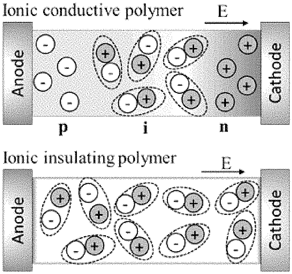
Single-layer LEDs were developed using a composite thin film of organometal halide perovskite (Pero) and poly (ethylene oxide) (PEO). Single-layer Pero LEDs have a device structure that resembles “bottom electrode (ITO)/Pero-PEO/top electrode (In/Ga or Au)”. Green emission LEDs with methylammonium lead bromide (bromide-Pero) and PEO composite thin films exhibit a low turn-on voltage of about 2.8-3.1 V (defined at 1 cd m−2 luminance), a maximum luminance of 4064 cd m−2 and a moderate maximum current efficiency of about 0.24-0.74 cd A−1. Blue and red emission LEDs have also been fabricated using Cl/Br or Br/I alloyed Pero-PEO composite thin films.

What is claimed is:

1. A single layer thin film optoelectronic device, comprising:

an anode;
a cathode;
a polycrystalline photoactive layer positioned between the anode and the cathode and wherein a first side of the polycrystalline photoactive layer is adjacent to the anode and a second side of the polycrystalline photoactive layer is adjacent to the cathode; and
wherein the polycrystalline photoactive layer comprises a methylammonium lead halide (CH3NH3PbX) deposited from a mixture of methylammonium halide (CR3NH3X) and lead halide (PbX2) and ion-conducting polymer (ICP) in a solution of dimethylformamide or dimethylsulfoxide, and thermally annealed, and wherein the relative weight ratio of the ICP over the total weight of methylammonium halide and lead halide in the mixture is sufficient to facilitate migration of cations towards the cathode and anions toward the anode, resulting in formation of a p-i-n junction in the polycrystalline photoactive layer.
2. The device of claim 1, wherein the ICP comprises poly(ethylene oxide).
3. The device of claim 1, wherein a molar ratio of lead halide to methylammonium halide in the mixture is approximately 1:1.5.
4. The device of claim 1, wherein X comprises fluoride (F), chloride (Cl), bromide (Br), iodide (I), astatide (At), or mixtures thereof.

5. A single layer thin film optoelectronic device, comprising:

an anode;
a cathode;
a polycrystalline photoactive layer positioned between the anode and the cathode and wherein a first side of the polycrystalline photoactive layer is adjacent to and in contact with the anode and a second side of the polycrystalline photoactive layer is adjacent to and in contact with the cathode; and
wherein the polycrystalline photoactive layer comprises an organometal halide perovskite (Pero) and an ion-conducting polymer (ICP), wherein the Pero is dispersed in the ICP, and wherein the relative weight ratio of the ICP over the weight of the Pero in the polycrystalline photoactive layer is sufficient to facilitate migration of cations towards the cathode and anions toward the anode, resulting in formation of a p-i-n junction in the polycrystalline photoactive layer.
6. The optoelectronic device of claim 5, wherein the Pero comprises a mixture of AX and BX, where A is a cation, B is a metal, and X is a halide ion.
7. The optoelectronic device of claim 6, wherein A comprises methylammonium (CH3NH3), formamidinium (NH2CHNH2), cesium (Cs), or mixtures thereof.
8. The optoelectronic device of claim 6, wherein B comprises lead (Pb), tin (Sn), germanium (Ge), or mixtures thereof.
9. The optoelectronic device of claim 6, wherein X comprises fluoride (F), chloride (Cl), bromide (Br), iodide (I), astatide (At), or mixtures thereof.
10. The optoelectronic device of claim 6, the Pero comprises AX and BX in a ratio of approximately 1.5 mole AX to 1 mole BX.
11. The optoelectronic device of claim 5, wherein the ICP comprises oligomers or polymers of ethylene oxide, a polysaccharide polymer, or a conjugated polymer.
12. The optoelectronic device of claim 5, wherein the Pero comprises methylammonium lead halide (CH3NH3PbX3), formamidinium lead halide (NH2CHNH2PbX3), cesium lead halide (CsPbX3), or mixtures thereof, wherein X is a halide.

13. A single layer thin film optoelectronic device, comprising:

an anode;
a cathode;
a polycrystalline photoactive layer positioned between the anode and the cathode and wherein a first side of the polycrystalline photoactive layer is adjacent to and in contact with the anode and a second side of the polycrystalline photoactive layer is adjacent to and in contact with the cathode; and
wherein the polycrystalline photoactive layer comprises an organometal halide perovskite (Pero) and an ion-conducting polymer (ICP), and wherein the relative weight ratio of the ICP over the weight of the Pero in the polycrystalline photoactive layer is sufficient to facilitate migration of cations towards the cathode and anions toward the anode, resulting in formation of a p-i-n junction in the polycrystalline photoactive layer, wherein the relative weight ratio of the ICP over the weight of the Pero is between about 5% and about 75%.

Share

Title

Single-layer light-emitting diodes using organometallic halide perovskite/ionic-conducting polymer composite

Inventor(s)

Zhibin Yu, Junqiang Li, Sri Ganesh Rohit Bade

Assignee(s)

Florida State University Research Foundation Inc

Patent #

10903441

Patent Date

January 26, 2021

Inquire about this intellectual property

Learn more about "Light Up the Future with Revolutionary Single-Layer LEDs"